
(At Jian Guo Hotel, Xi'an CHINA)
| CEEM '96 Nov. 5-7 1996 Xi'an CHINA |
筐体内に配置した多層プリント回路のサセプティビリティ
小暮裕明、中野英樹、越地耕二、周英明
(CEEM '96 Nov. 5-7 1996 Xi'an CHINA)
"Susceptibility of Multilayer Printed Circuit inside Equipment Housing"
Hiroaki KOGURE, Hideki NAKANO, Kohji KOSHIJI and Eimei SHU
CEEM(Asia-Pacific Conference on Environmental Electromagnetics)
(At Jian Guo Hotel, Xi'an CHINA)

(The South Gate, ancient capital of CHINA)
INTRODUCTION Recently we spent too much to re-design circuits and fabrications because of the requirements of large integration and the multilayer printed circuit. It is so difficult to measure characteristics between the layers especially a smaller multilayered structure.
The circuit theory gives less accurate answers in these structures. This paper deals with the electromagnetic field analyses for susceptibility of the multilayer printed circuit board (PCB) inside the equipment housing using EM analyses, Sonnet "Em" by the Method of Moments and KCC "Micro-Stripes" by the Transmission-Line Modeling Method.
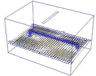
MODELING OF THE PROBLEM It is so useful to analyze characteristics of multilayer PCB by modeling three dimensional structure. The three layered PCB (x=260mm, z=180mm) consists of signal line at a top layer #1, ground plane at a middle #2 and Vcc at a bottom #3. One edge of the line is connected to #3 through via and another to #2 with 50 Ohms termination. This PCB is located at lower center of the equipment housing cubicle (x=300mm, y=150mm, z=200mm). It has a thin slot(10mm wide, 100mm long) at a center of the top plate and a plane wave is excited 50mm above the slot. In another case, a short cable such as a power supply which led to inside the housing is also modeled.
SIMULATION RESULTS The electric and magnetic field 50mm above the PCB shows TE mode resonance assuming that the cubicle acts like a rectangular cavity resonator. It has four resonant frequency up to 2GHz because the PCB itself partition the cubicle into upper and lower room.
The induced current at a signal line by the plane wave excitation shows maximum level when the line is located at the edge of the PCB, excited x direction with a slot of z direction. And the minimum case is the line at the center, excited with a slot of both z direction. The latter shows over 20dB lower than former up to 2GHz and this is found to the best location for susceptibility of the PCB inside the equipment housing. The difference of induced current between a single ground plane and multilayer PCB is rather small from 1GHz to 2GHz, but the former shows 10dB lower up to 400MHz.
In the latter case the ground plane is connected to the side wall at six points. The induced current shows approximately 5dB lower up to 1GHz, but it cause some peak level of 20dB higher at 700MHz, 800MHz, 1GHz, respectively.
The reason of this resonance seems to be different. In the lower frequency, the surface current distribution shows the high current which flows along the edge of the ground plane and the side wall connected by the thin metal. The other case results the resonance between the ground plane and Vcc has been dominated.
A short cable of only 30mm which lies outside the housing is also modeled. The induced current shows approximately 20dB lower than the case through a slot up to 2GHz, but it can be found the same higher level at the particular frequency up to 500MHz.
CONCLUSION These two different algorithm made good agreements and could be recognized to produce many useful basic information for evaluation of susceptibility. The coupling to the circuits inside the equipment housing through a thin slot and the coupling by a cable led to inside the housing are analyzed.
